
A MM PHONO vacuum tube preamplifier
Circuit diagram and LTspice simulations
My prototype
Measurements
A few months later: anti-bump circuit
Conclusion
WARNING: vacuum tube circuits like this preamplifier require high voltages. There is a shock hazard when the circuit is on and for several minutes after it has been switched off, since capacitors store some charge for a while. A lack of attention may have lethal consequences. Builders must be very well aware of all safety rules which must be applied.
Introduction
For Christmas 2014 I was given a turntable. It may seem strange to listen to vinyl records in 2015 (NOTE: now in December 2022 vinyl records are widespread again), but I inherited a collection from my father. Spinning records reminds when we listened to music together when I was a kid. So, I practically grew up with Pink Floyd, Italian progressive rock (Banco del mutuo soccorso, PFM) and a lot of classical music in my ears. By the way, we were happy when we adopted CD, but this is another story.
My new turntable is an Akai ATT05U. It is one of those USB turntables, it is reasonably well built, belt-driven and equipped with an internal amplifier which can be easily bypassed. I equipped it with a good cartridge (Audio Technica AT440MLa, shown in figure 1) and it sounds fine. I do not think that vinyls sound better than CD's or other (good quality) digital counterparts, but I really enjoy taking care of them and spending time trimming the turntable the best I can. I do not think that something is bad just because it is old. Playing vinyl records is a different experience from playing a CD or a mp3 and I like it. A record is a beautifully crafted object and a turntable is based on both simple and very refined physical principles. I discovered with pleasure that there is in this moment a vinyl revival and it is very easy to find new and second hand records in stores.
I built a few years ago a power amplifier, as described in this page. I am fully satisfied of it: it is adequately powerful, rugged and very effective with my loudspeakers. I have a CD player and a turntable: I needed at least something to select the source I want. I thought it was time to employ some of the vacuum tubes I had lying around for some years. I have been satisfied with the results and in this webpage, I describe my simple preamplifier based on vacuum tubes, equipped with a RIAA phono stage for moving magnet (MM) cartridges. It allows selecting different loads for the cartridge and it is based on two ECC83/12AX7A double triodes, with an output stage based on a ECC88/6DJ8 double triode.
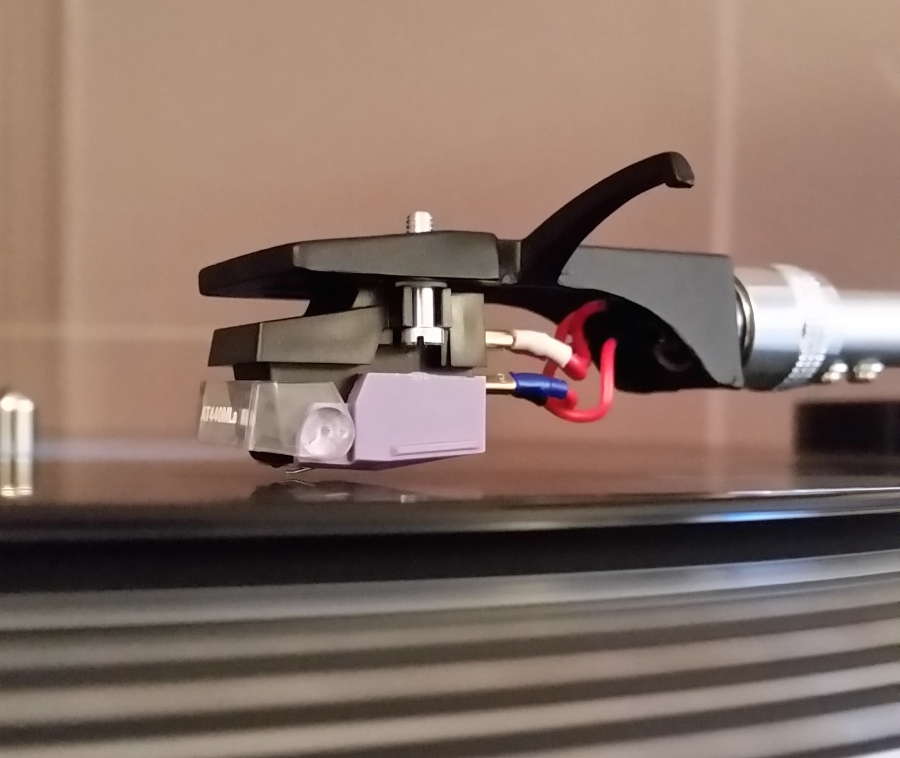
Fig. 1: the Audio Technica AT440MLa softly grooving (click to enlarge).
I do not think vacuum tubes have any kind of "sonic superiority" or other sorts of magical advantages against discrete transistors or operational amplifiers. They simply follow the laws of physics, as everything else. However, I have a taste for vintage circuits and I wanted to see what I could build. As a side note, I was hesitant for a while if it was worth adding a Baxandall-like tone control. I finally decided it would not have been useful, given the performances of the power amplifier and loudspeakers. Therefore, my circuit does not include any form of tone controls (except, of course the RIAA equalization network for the PHONO inputs). I do not have any tape deck, so I left out the tape in/out circuitry.
This document is organized as follows. At first, I will briefly discuss the circuit diagram and the technical solutions adopted. Then, for the RIAA PHONO input stage, I will provide simulation results obtained with LTspice. I will successively describe my prototype and I will spend some time to present measurement results. In particular, I will focus on the compliance with the RIAA equalization curve, noise floor and hum levels and finally the harmonic distortion of the stages. I will end the article with a conclusion.
Circuit diagram and LTspice simulations
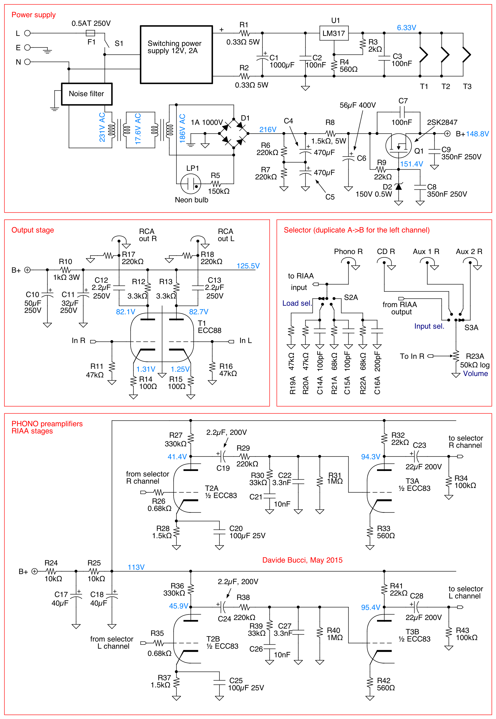
Fig. 2: the schematic, drawn with FidoCadJ. Measured voltages are DC, referred to the ground, except for AC supplies (click to enlarge).
The circuit diagram of the preamplifier is visible in the figure 2 and is available in the FidoCadJ file format (if you do not know what FidoCadJ is, have a look here). It is composed by a power supply for the anodic voltages (B+), as well for the filaments, the input PHONO/RIAA stage, an output stage as well as a selector.
Simulating the RIAA PHONO preamplifier
The most delicate part of the circuit is of course the RIAA phono preamplifier, which is built around T2 and T3, both ECC83/12AX7A vacuum tubes (valves). Each one is a double triode and I built very simple common-cathode amplifiers around each of them. The configuration provides a sufficient amount of voltage gain and the RIAA-equalization network is based on R29-R31, C21 and C22 for the right channel and R38-R40, C26 and C27 for the left channel. So, I ran some LTspice simulations on the circuit shown in figure 3, where the bias voltages are shown. I used the the triode models from Duncan Amps website, which include the ECC83/12AX7A tube.
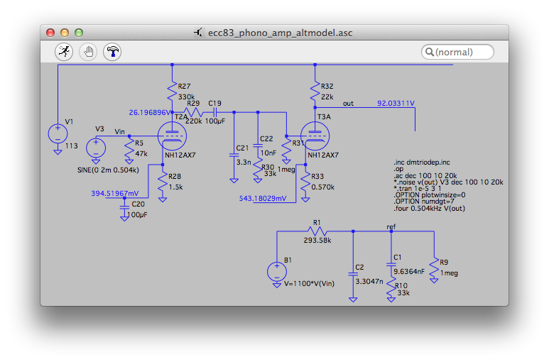
Fig. 3: the PHONO amplifier with the RIAA network in LTspice. The network at the bottom is used as a reference.
Comparing figures 2 and 3, it appears that the plate voltages are predicted in a quite accurate way by the simulation for T3. Since T2 works on a quite low plate current (around 0.22 mA), probably the accuracy of the computer models becomes questionable. It is also possible that the ECC83 I employed has already been used in the past and shows some marginal signs of wear.
The RIAA equalization network is calculated to introduce two poles at 50 Hz and 2122 Hz and a zero at 500 Hz in the transfer function. These correspond to the time constants of the standard RIAA equalization, which are respectively 3.180 ms, 75 μs and 318 μs. I first calculated analytically the values of the components in the equalization network, using elementary models for vacuum tubes. I then checked the correctness of the RIAA circuit using LTspice. The values have been tweaked so that a better result could be obtained. Even with standard components of the E24 series for the resistors and E12 series for capacitors, the difference from the standard RIAA curve is below ± 0.1 dB, as visible in figures 4. Two curves are represented: the transfer function of the circuit, built with components of the E24 series and the transfer function of a network with ideal components. The 0.4 dB shift between the two curves is due to the arbitrary factor of source B1 in figure 3 and bears no importance. What counts is that all the differences remain in an interval of 0.2 dB, between -0.3 dB and -0.5 dB. Sensitivity from the tolerances can be estimated via a Monte Carlo simulation, but I leave that to the scrupulous reader.
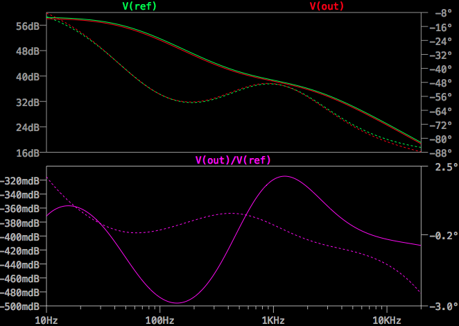
Fig. 4: above, simulated response with standard components (AC analysis, red) and theoretical (green) RIAA curve; magnitude and phase of circuits of figure 3. Below, ratio between response with E24 components and theoretical ones. BTW, I suffer every time I see capital "K" to indicate x1000 multiplier, instead of "k".
LTspice circuits are available for download here. Figure 5 shows the results of a 65536 points FFT calculated on a rectangular window for a sinusoidal signal at the output of the circuit. A 6 mV peak to peak sine at 1 kHz is injected in the input. The amplitude of the output signal is 0.48 V peak to peak and the distortion is mainly coming from the second harmonic. Fourier analysis indicates approximatively 0.041% of total harmonic distortion, a respectable figure, reasonably in the HiFi ballpark.
The wide dynamic range visible in figure 5 is a result of the increased precision of the calculations as well as the choice of a time interval of 2 s, containing an integer number of periods of the input 1 kHz signal. In a transient simulation to evaluate the harmonic distortion, do not forget to turn off the compression of the output data and reduce considerably the tolerance of the calculated data (but this yields longer simulations). Incorrect settings of LTspice would result in THD always around 2 or 3%; even for signals from purely sinusoidal voltage sources. The risk of computers is called GIGO: Garbage In, Garbage Out.
Distortion simulation can be repeated at a frequency of 504 Hz, since I will in fact measure the performances at that frequency. A simulation for a 6 mV peak to peak input sine at that frequency predicts an output signal of 0.64 V peak to peak, with a THD of 0.14%. Once the input signal is reduced so that the output amplitude is 0.48 V peak to peak, the distortion figure is reduced to the same 0.04% already obtained ad 1 kHz. As expected, THD greatly depends on the output amplitude and on the performances of T3.
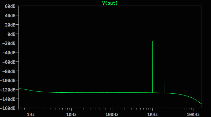
Fig. 5: magnitude of FFT of transient simulation of the output signal in the circuit of figure 3, with an input signal of 6 mV (peak to peak) at 1 kHz. Second harmonic is 68.7 dB below the fundamental tone, spectrum is remarkably numerical noise-free, because an integer number is comprised in the (rectangular) temporal window employed for the FFT.
Output circuit, power supply and other details
The output stage is built around an ECC88 and is another common cathode amplifier having a gain of approximatively 10 dB. Its output impedance is about 3 kΩ, which is low enough to drive any power amplifier. It is fed by the signals from the selector circuitry. For each section of the ECC88, the anodic current must be around 13 mA (much higher than for the phono stages). If a source which does not require amplification is chosen (such as a CD player), the volume potentiometer R23A/R23B plays only the role of a variable attenuator.
The power supply is a delicate matter, since using the common cathode configuration all the noise present in the power supply rails is automatically transferred to the signal. Therefore, I applied a consequent amount of filtering before and after a simple regulating stage built around a 150 V zener diode and a high voltage MOSFET. Q1 is a high-voltage N-channel MOSFET such as a 2SK2847 from Toshiba (I found it in an old CRT computer monitor). It should be able to withstand at least 250 V between source and drain and provide 1 A. The power dissipation is below 2 W, but a small heat sink is necessary.
I tried many solutions for energizing the filaments. At 300 mA required for each tube with 6.3 V supply strategy, we have around 900 mA in total. I would have adopted a 12 V power supply, permitted by the ECC83 tubes but not by ECC88. I noticed it is very important that the filaments are powered with a filtered DC signal. I therefore employed a switching power supply (from an old external hard disk box), followed by a filtering stage and U1, a LM317 integrated regulator. Unfortunately, the regulator must dissipate about 5 W and a heat sink is mandatory. I mounted everything inside the enclosure of the amplifier and I realized that everything tended to run too hot (the total heat dissipation of the complete circuit is about 20 W). I thus added a 12 V fan mounted on the top of the enclosure, right above the regulator heat sink. Powered at 6.3 V, the fan is silent enough to be used in this context.
Some components are quite critical and others are not at all. For example, I employed in the B+ filtering several capacitors I savaged from old tube equipments (of course, I checked them carefully to be sure they were functional). So, instead of C10 and C11 which have the nonstandard values of 50 μF and 32 μF, one can employ any electrolytic capacitor able to withstand at least 200 V and above 30 μF. The same can be said for C17 and C18. Instead, quite critical for the RIAA time constants are capacitors C21, C22, C26 and C27 and resistors R27-R31 and R36-R40. Those components does not need to have a high voltage rating. Feel free to change the cartridge loading resistors and capacitors around S2A (and S2B). In my case I put the values I wanted to test with my cartridge.
My prototype

Fig. 6: the prototype I built using a copper clad and air wiring techniques, without the anti-bump circuit (click to enlarge).
I built my prototype soldering the components on a copper clad base. The vacuum tubes are mounted horizontally, soldering the passive components directly on the back of the noval sockets. Much attention has been devoted to the ground plane, everywhere, making sort that it remains as electrically clean from noise as possible. In principle, I ensured that all ground connections are organized in a star-like topology from the filter capacitors of the power supply. No high current path is present in the ground plane and for example the filament supply is provided by two wires which are kept separate from the ground plane. In order to make sort that the ground connections adopt a star configuration, for example, the ground connection of each RCA connector in the back panel is not connected to the panel itself and it is physically kept separate until the shielded cable reaches the switch in the front panel.
When building the prototype, I went through some unexpected problems. For example, I realized that there was a tendency of the circuit to oscillate to a very low frequency (this is called motorboating). I noticed that there was a coupling through the power supply between the RIAA preamplifier and the output stage built around T1. This was due to a simplistic filtering strategy adopted: the RC stages which must be kept well separate between the different stages. A second unexpected problem was the tendency of the Q1 MOSFET to self-oscillate on some particular conditions of voltages and currents. From a practical point of view, this manifested by a very loud 50 Hz hum for one or two minutes when switching on the preamplifier. When I noticed that the hum came from very fast spikes synchronized with the 50 Hz mains, I spent some time thinking that the tubes were oscillating! Oscillation was tamed by adding C7 a 100 nF capacitor between the source and the drain of Q1 (I will maybe try to reduce it).
It is mandatory to shield adequately everything and therefore to adopt a metallic enclosure for all the circuit. A screen should be employed for T2, which is amplifying the most delicate signals. Even if the cables are shielded, delicate signals should never be routed close to the transformers or wires carrying AC voltages.
Measurements
RIAA equalization
There are several measurements which can be done on a PHONO preamplifier. For example, it may be interesting to see what is the overall transfer function, to check the compliance with the RIAA standard. Then, one might try to measure the characteristics of the noise floor of the preamplifier and the total harmonic distortion. My laboratory includes a Brüel&Kjær dual channel FFT spectrum analyzer, model 2034. It is a vintage equipment, but it is still very useful tool for audio signals. The first thing I did was to acquire the transfer function of one channel, from PHONO to OUT with the volume potentiometer at the maximum level. Measuring a transfer function can be done employing a pseudo-random noise generated by the instrument at the input and inspecting at the same time the input and the output of the amplifier with the two channels of the spectrum analyzer. Dual spectrum analyzers can implement very refined strategies for obtaining transfer functions of equipments employing an almost arbitrary signal (see for example Dual channel FFT analysis, part I and Dual channel FFT analysis, part II by H. Herlufsen, in the Brüel&Kjær library).
Most of the measurements shown in this page have been done with a Hanning windowing function (except where explicitly indicated otherwise) and optimizing the sensitivity of the inputs, without having saturation or being close to the noise floor of the instrument. Since the signal level of the internal signal generator of the 2034 is too large for feeding directly the PHONO input, I employed an attenuator made by a 120 kΩ resistor in series to a 0.68 kΩ resistor. Connected to the output of the 2034 and to the input of the preamplifier (47 kΩ load), I measured an attenuation equal to -45.3 dB within ± 0.1 dB between 0 Hz and 25.5 kHz. Once the transfer function of the whole preamplifier has been measured, the influence of the attenuator has been memorized and compensated ("equalized") by the instrument, with an average of more than 50. Therefore, the screenshot shown in figure 7 depicts directly the magnitude of the transfer function of the preamplifier.

Fig. 7: transfer function of the preamplifier, PHONO to OUT at max volume. Logarithmic frequency scale, from 256 Hz to 25.5 kHz, vertical range of 40 dB (click to enlarge).
A few words about how to read the B&K 2034 screen. The horizontal axis spans from 256 Hz and 25.5 kHz and is logarithmic. Vertical lines represent the measured FFT bins (each one covering 32 Hz in this configuration) and clearer lines are traced every 1000 Hz. The vertical axis is in dB, the whole span is 40 dB and therefore a major division is 5 dB and a minor one 1 dB. The level at the top of the screen represents a 60 dB amplification, therefore at the bottom we have 20 dB. The cursor is at 256 Hz and gives a reading of 58.2 dB.
| Frequency | Theoretical RIAA | Measured |
|---|---|---|
| 24 Hz | 19.0 dB | 19.0 dB |
| 48 Hz | 17.1 dB | 17.1 dB |
| 64 Hz | 15.7 dB | 15.7 dB |
| 104 Hz | 12.8 dB | 12.7 dB |
| 152 Hz | 10.1 dB | 10.1 dB |
| 200 Hz | 8.2 dB | 8.1 dB |
| 304 Hz | 5.4 dB | 5.2 dB |
| 504 Hz | 2.6 dB | 2.6 dB |
| 1000 Hz | 0.0 dB | 0.0 dB |
| 1504 Hz | -1.4 dB | -1.4 dB |
| 3000 Hz | -4.8 dB | -4.9 dB |
| 5000 Hz | -8.3 dB | -8.6 dB |
| 60000 Hz | -9.6 dB | -9.9 dB |
Tab. 1: comparison between theoretical and measured RIAA curves, normalized to 0.0 dB at 1 kHz.
Table 1 shows the measurement results done on the PHONO/RIAA stage (i.e. the input was the grids of T2 and the output was taken after the decoupling capacitors on the plates of T3). The measurements have been done using the spectrum analyzer and normalizing the data to the amplification got at 1 kHz. The uncertainty of measured data is due to the B&K 2034 and can be evaluated at ± 0.2 dB A similar normalization to the theoretical curve calculated by LTspice has been done. The similarity between the theoretical data and the measured ones is simply amazing. This means that LTspice simulations correctly evaluate the output resistance of the ECC83, as well as its internal capacitances.
Triode models does not include noise data. Therefore, noise analysis would yield unrealistically optimistic noise levels, taking into account only the contributions from resistances.
Noise floor and hum
Measuring the noise floor requires a different setup. A single channel spectrum averaging acquisition has been done, on a frequency range below 6.4 kHz, shorting together the PHONO input with the ground. The measurements have been repeated twice. At the first time with the volume to the maximum level to determine the performances dominated via the input RIAA stages around T2 and T3 (ECC83). Then, by reducing the volume to the minimum, to see the performances of the output stage built around T1. The screenshot reported in figure 8 shows the results acquired by the B&K 2034, in the first situation.
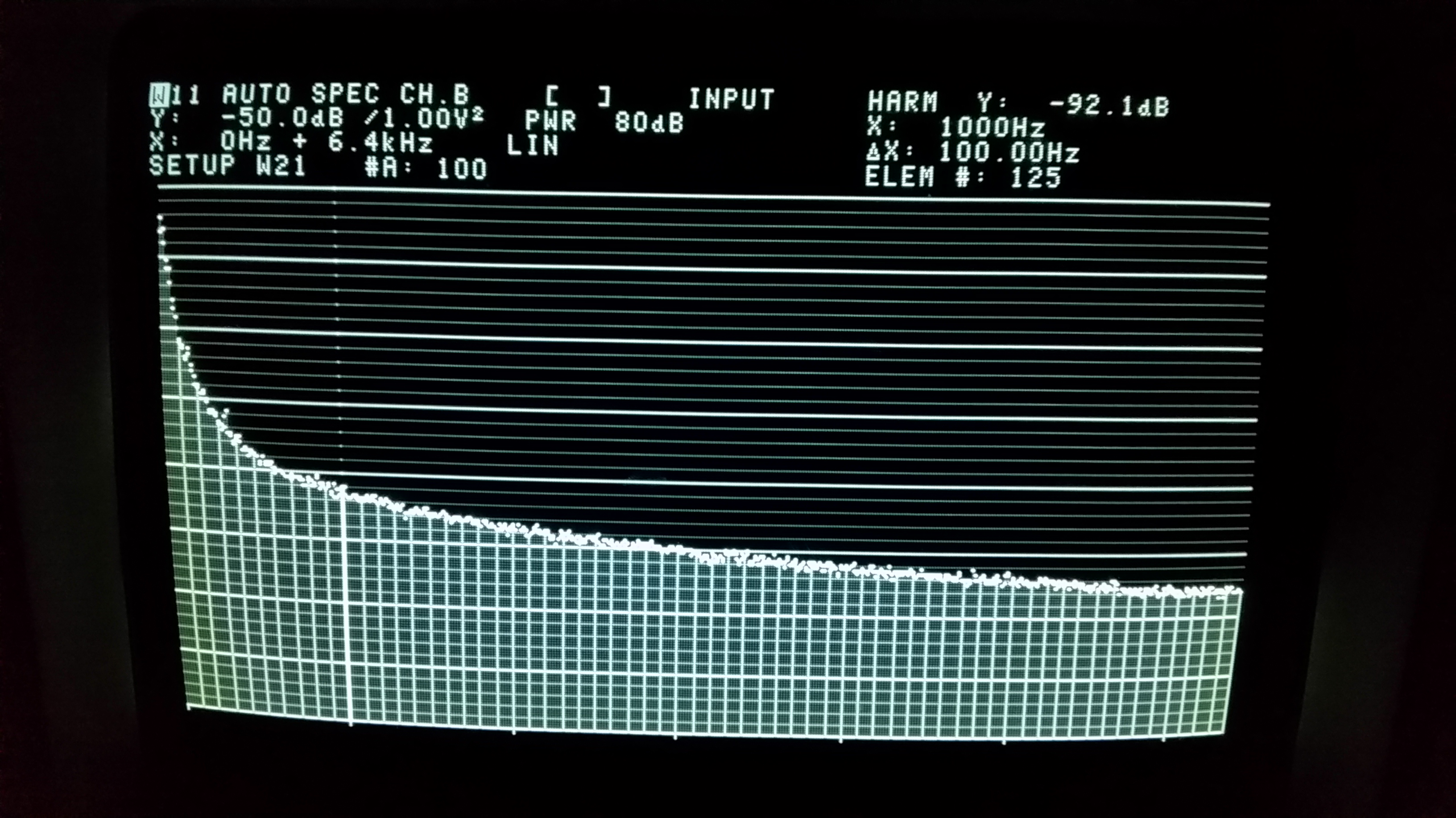
Fig. 8: noise floor of the preamplifier, measured below 6.4 kHz at the output of the preamplifier, with volume at the maximum level and shorted input. Noise from the PHONO/RIAA stage dominates (click to enlarge).
In this measurement, the frequency scale is linear, the clear lines indicates multiples of 100 Hz and the cursor is placed at 1 kHz. The instrument shows the power measurement of each 8 Hz FFT bin (retrospectively, I think that I may have configured it to show a power spectral density (PSD) estimation, but the only difference would have been in the measurement units).
First of all, no signals at multiple of 50 Hz can be spotted, indicating that hum residue is below the noise of the circuit. An oscilloscope observation shows that a tiny amount of (<1 mV) switching noise at 30 kHz is still there, albeit inaudible. Then, the RIAA equalization network appears to shape the noise and an increase at low frequency is apparent. At low frequency, the vacuum tube also exhibits a higher flicker (1/f) noise in addition to the Johnson (thermal) noise.
Turning the volume to the minimum allows to measure the performances of the output stage, as shown in picture 9.
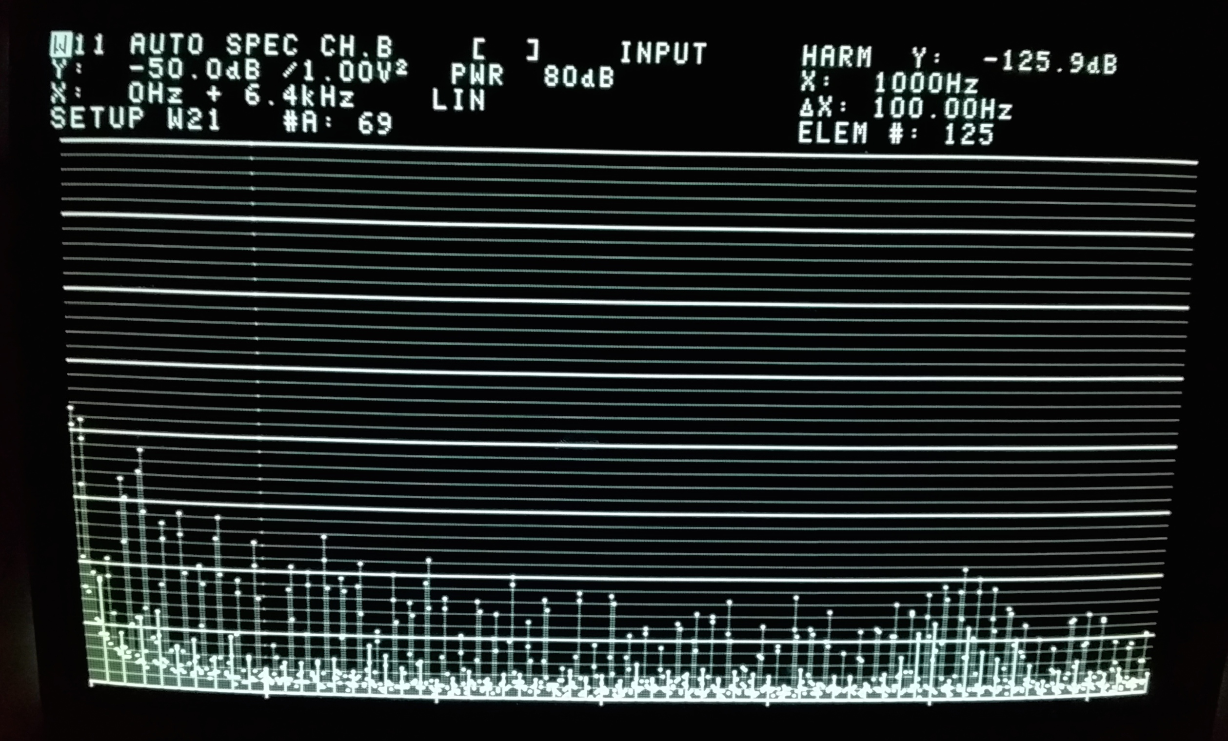
Fig. 9: noise floor of the output stage, measured below 6.4 kHz at the output of the preamplifier, with volume at the minimum level and shorted input. Noise and hum from the output stage is distinguishable (click to enlarge).
Now, the presence of a tiny amount of hum is clearly visibile, tending to manifest itself in spectral components at odd multiples of 50 Hz. The scale of figure 9 is the same employed in figure 8: a pure tone with an amplitude of 1 V RMS would be 50 dB above the top of the scale, the total range shown being 80 dB. Those might be reduced probably by tweaking the position of the output cables and the filtering of the power supply. However, the hum level is below the one already introduced by my power amplifier (I barely hear it by putting my ear close to the woofers), so I decided it was acceptable for my needs. Moreover, in those conditions, the amount of hum in the loudspeakers depends more on the quality of the wiring between the turntable, the amplifiers and the loudspeakers. All of those are factors external to the preamplifier itself.
Harmonic distortion at 504 Hz
Measuring the Total Harmonic Distortion (THD) is done by feeding the preamplifier with a spectrally very pure signal and measuring the spectrum of the output signal. I have built in the past a little Wien-bridge oscillator, giving a 504 Hz tone with a THD below 0.01%. The signal from the oscillator has been attenuated by 45 dB with the same strategy seen above and used to fed the PHONO input. In a first test, the output signal has been taken after the decoupling capacitor of T3, therefore giving an idea of the performances of the RIAA phono stage. The goal being to compare results with the ones simulated above, and the signal amplitude was set so that 0.48 V peak to peak (-15.4 dB to a reference of 1 V RMS) is obtained at the plate of T3. Figure 10 shows the results of a typical measurement, done with the B&K 2034 in a single channel mode, flat-top windowing function and a span of 1.6 kHz.
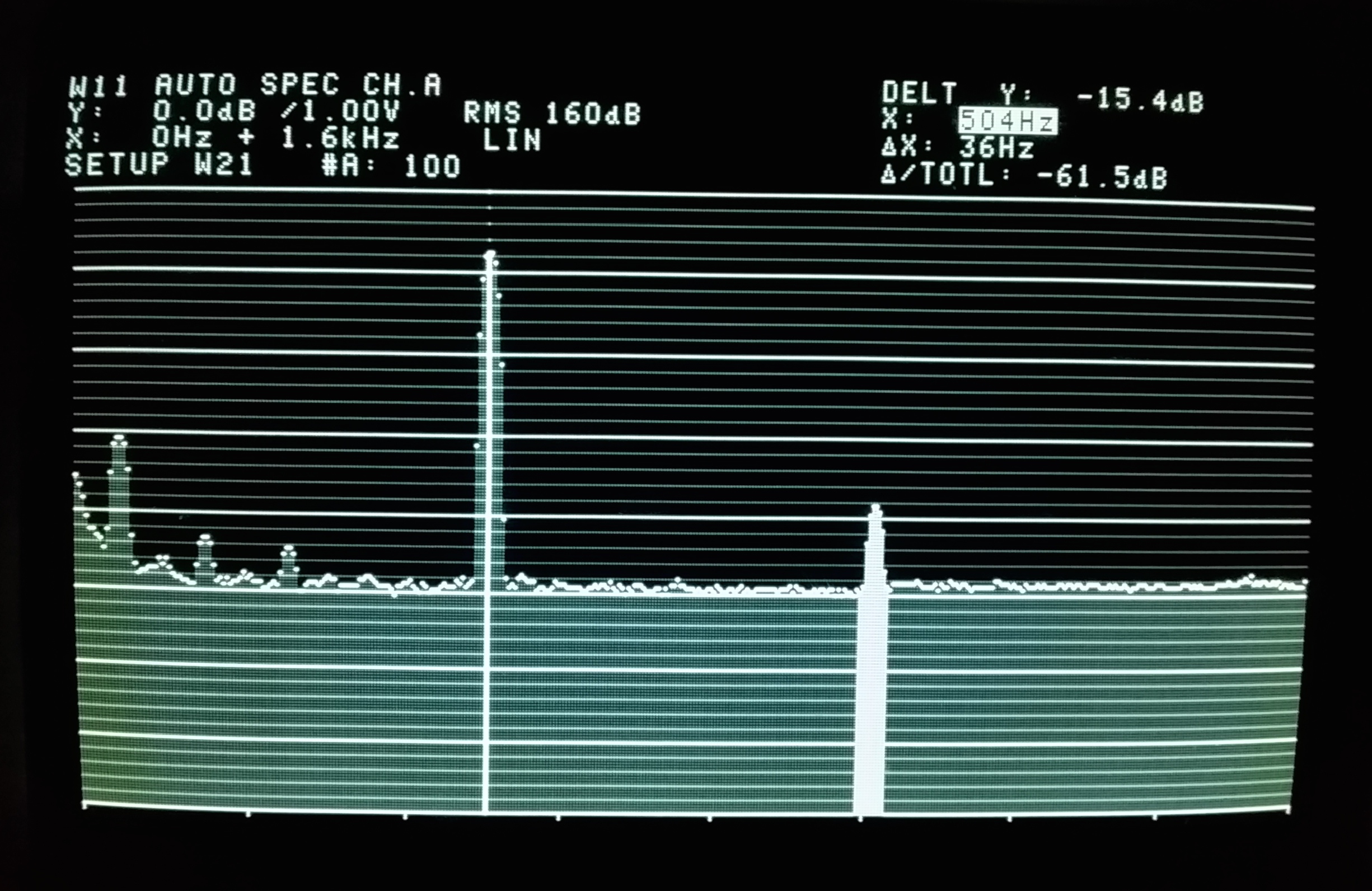
Fig. 10: Spectral analysis of the output signal of the riaa/phono stage, fed by a very pure 504 Hz test tone (click to enlarge).
The vertical axis of figure 10 spans 160 dB and the noise floor of the spectrum analyzer is clearly visible. The level of the second harmonic is 63 dB below the fundamental at 504 Hz, with a third harmonic which is barely visible on the noise floor. This represents a THD of 0.07%, which is reasonably agreeing with the simulation results. It is worth noticing that I own several ECC83's (built by RCA in the USA, they are marked 12AX7A and the date code suggests that they were built around May and June 1962). Therefore, I tried several of them, especially for T3 and I selected the tubes yielding the lowest THD. Difference are notable and for some of them the distortion could approach 0.2%. I do not know the story of the tubes and it may be that the worst performers were indeed a little worn out. Indeed, those tubes also gave bias points quite far from the ones calculated by LTspice and shown in figure 3. However, it is clear that differences between tubes are indeed easily measurable.
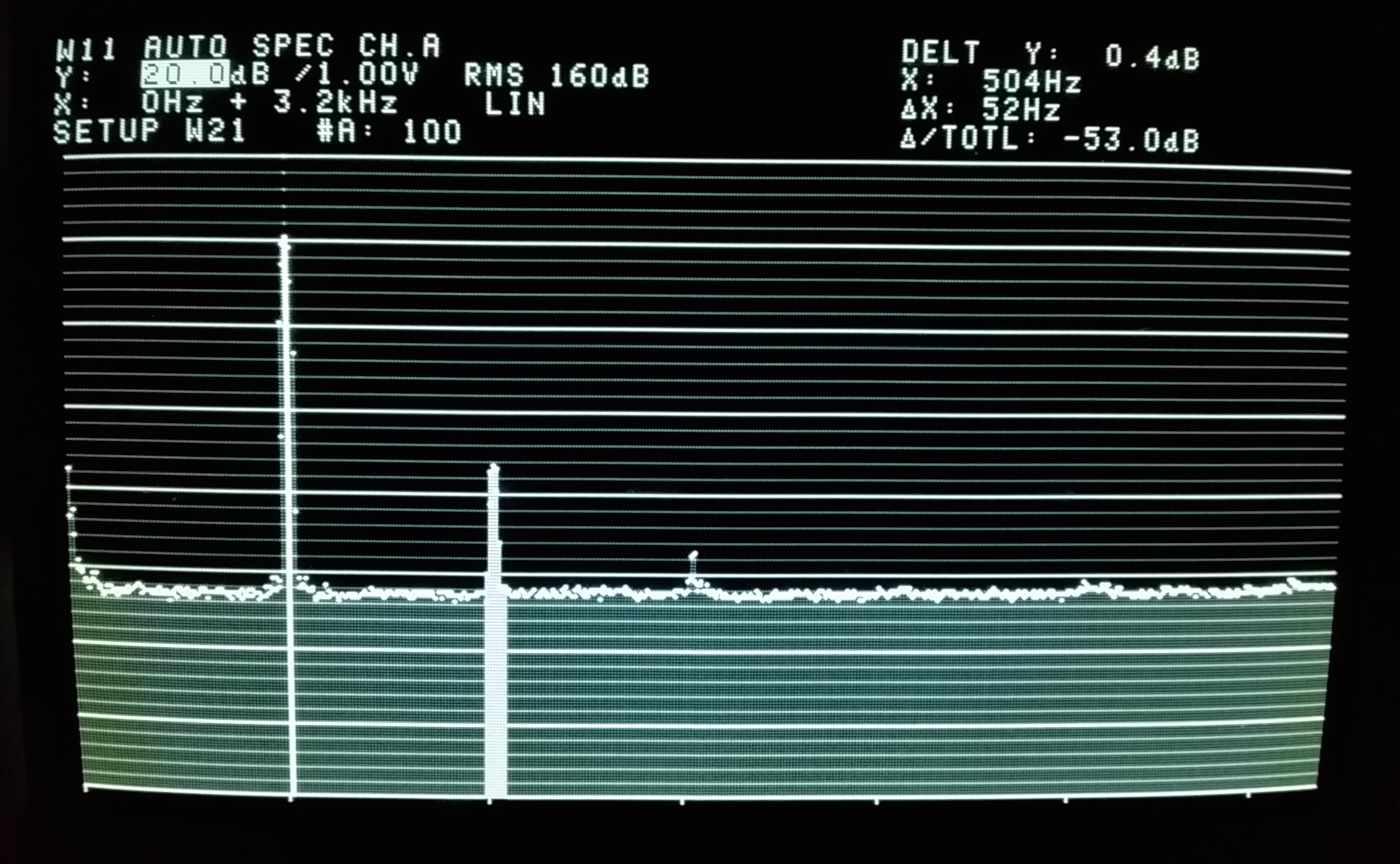
Fig. 11: Spectral analysis of the output signal of the output stage, fed by a very pure 504 Hz test tone, the horizontal scale spans from 0 to 3.2 kHz (click to enlarge).
Figure 11 shows the spectrum of the output signal when the same 504 Hz test tone is fed by the CD input, with an amplitude such that the output signal is a little above 1 V RMS, which means 2.83 V peak to peak. The distortion coming from the second harmonic is estimated around -53.0 dB, corresponding to 0.22%, with the third harmonic about 20 dB below. This is a rather extreme situation, since my power amplifier in this condition would try to slam more than 23 V RMS to the 8 Ω loudspeaker (and without success: this would yield 66 W of average power, already above its saturation level).
Frequency response of the CD/AUX inputs, output impedance
Measuring the frequency response is comparatively an easy task. I built recently an AC millivoltmeter. Employing a signal generator, I injected a sine voltage at 1 kHz in the CD input, by setting the output amplitude so that I obtained 200 mV peak to peak at the output. The output was loaded on a 47 kΩ resistor. Then, I changed the frequency until a reduction of 1 dB could be detected (thus the output signal would be reduced 178 mV peak to peak). I obtained 40 kHz ± 2 kHz for the upper range. The lower range was probably around 2 Hz, but I was limited by the bandpass of my AC millivoltmeter and I would indicate 5 Hz as a conservative value.
To measure the output impedance (which I expected to be below 3 kΩ), I measured the output signal of the preamplifier and then I attached a 5 kΩ potentiometer, searching the setting point which gave a reduction of 50% of the output signal. Measuring the resistance which corresponded to that point, I obtained (2.3±0.2) kΩ, low enough to drive any power amplifier.
| Parameter | PHONO input | CD/AUX inputs |
|---|---|---|
| Equalization | ± 0.3 dB from RIAA curve below 6 kHz | Flat |
| Gain at 1 kHz (max. volume) | (53.7±0.5) dB | (21.2±0.2) dB |
| Gain at 32 Hz (max. volume) | (69.1±0.5) dB | (21.2±0.2) dB |
| Gain at 10 kHz (max. volume) | (39.6±0.5) dB | (21.2±0.2) dB |
| Phase | 180° + RIAA equalization | 180° |
| -1 dB frequency response (47 kΩ load) | n.a. | 5 Hz to 40 kHz |
| Harmonic distortion at 504 Hz | 0.07% with output of T2 at 0.48 V pk/pk | 0.22% with output of T1 at 2.48 V pk/pk |
| Input impedance | 47 kΩ or 68 kΩ (additional 0, 100, 200 pF) | 47 kΩ |
| Output resistance | (2.3±0.2) kΩ | (2.3±0.2) kΩ |
Tab. 2: summary of characteristics of the preamplifier. Measured values are in boldface.
A few months later: anti-bump circuit
When I am writing those lines, I used this preamplifier almost daily since I built it and I can say that I am quite pleased by its performances. However, a particular problem must be discussed and solved.
Indeed, I observed that in my setup the preamplifier must be switched on and off only when the power amplifier is off. In fact, if this is not done, a very loud bang was sent to my poor loudspeakers. To be on the safe side, I had to switch on the preamplifier, wait half a minute and then switch on the power amplifier. The switch off sequence is reversed: at first the power amplifier and then the preamplifier, after a few seconds.
Having a look at the circuit shown in figure 2, the origin of the problem becomes clear. In fact, when switching on the circuit the B+ voltage is readily present, before the tubes's filaments are hot. Therefore, the voltage on T1's plates at first follows in practice the transient of the B+ voltage.
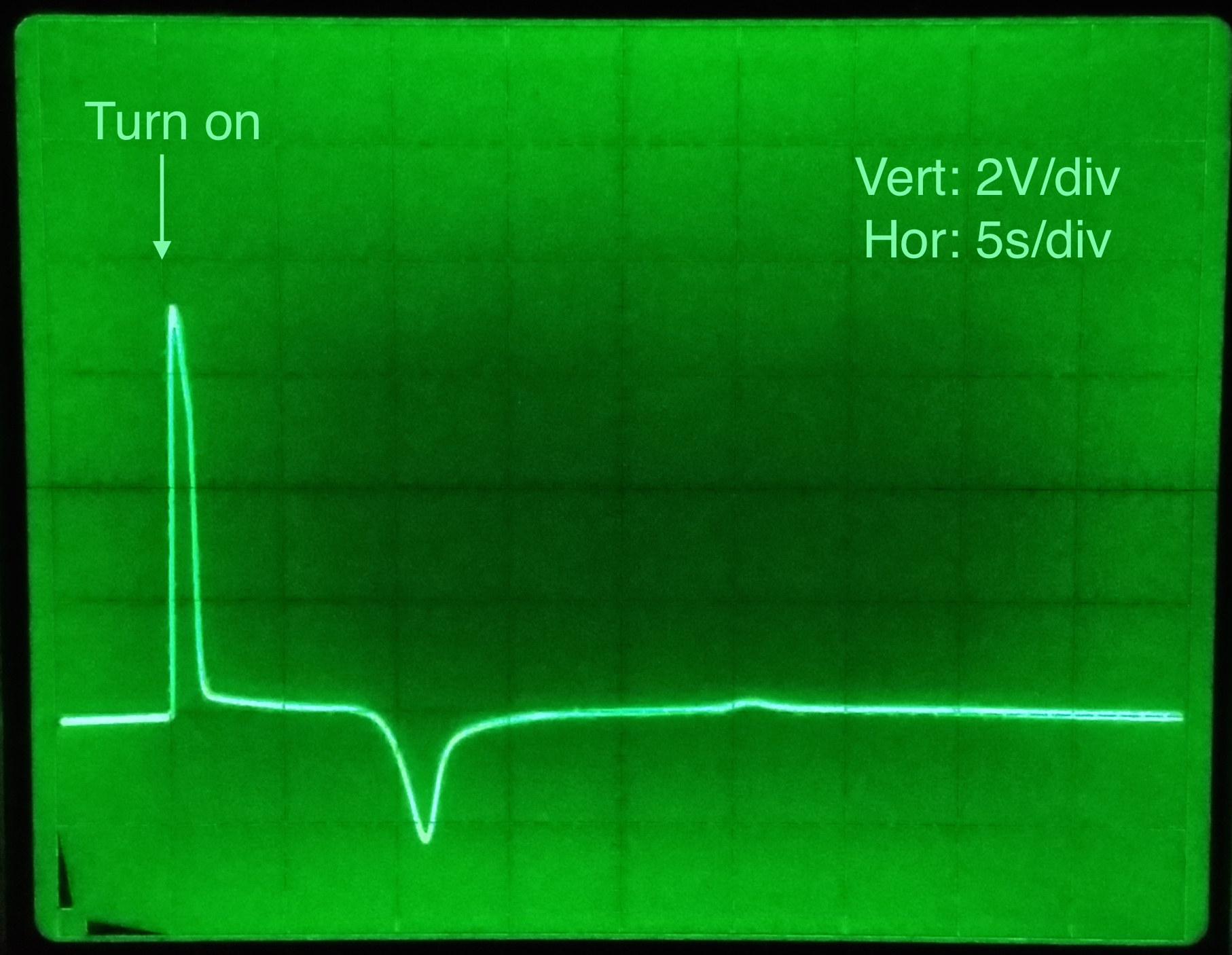
Fig. 12: switching on transient, with a 47 kΩ load on the output. I love the vintage analog memory of oscilloscopes! (click to enlarge).
This transient is relatively fast... and passes through the C12 and C13 capacitors (they cut the DC component, but here we are not yet there!) and is coupled on the output. Right at the input of the power amplifier! We have quite large voltage swings here: BOOM! After a wile, the cathodes of the vacuum tubes are hot enough and the voltages on the plates drops, to gradually approach the working point. This transient can also pass through C12 and C13. Figure 12 shows the turn on transient. We can see there the positive peak immediately after the switch on, followed by a negative peak around ten seconds later and a last small grunt at around 25 s. The peak to peak amplitude of that transient is about 10 V: more than enough to saturate my poor power amplifier! A common cathode output would probably have been less subjected to this issue (even if the problem would not be completely solved).
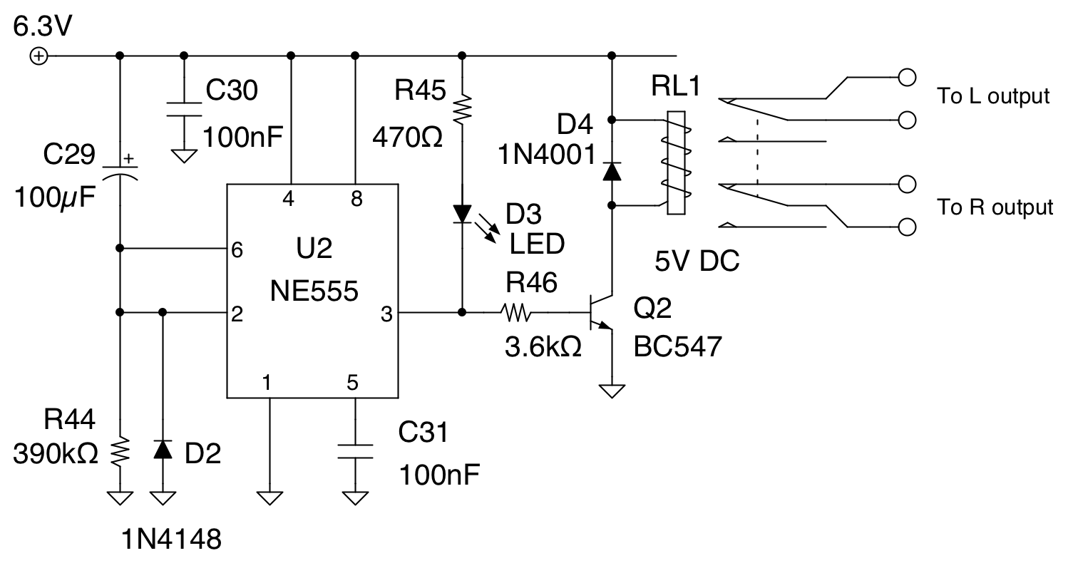
Fig. 13: the anti-bump circuit (click to enlarge).
A solution can be however easily found, with a small delay circuit which can safely keep shorted the outputs of the preamplifier for a safe delay at the turn on. When the amplifier is switched off, the outputs must also be shorted very rapidly. The solution shown in figure 13 is based on the classic NE555 timer, employed as a very simple delay circuit which controls a DPDT relay. The FidoCadJ version of the schematic is available. The relay must be connected to the outputs in such a way they are shorted when the coil is not energized. The delay is set by the values of capacitor C29 and resistance R44. The values shown give a delay of about 35 s with a traditional non-CMOS NE555 integrated circuit. I have employed D3, a white LED which turns on when the circuit is... waiting! My LED requires quite a small current and this explains the relatively high value of the resistance R45 for a 6.3 V power supply. The circuit can be powered by the filament supply rail of figure 2.
NOTE: from 2016 to Nov. 15, 2020, the circuit shown in figure 13 contained an error (D2 was connected upside down).

Fig. 14: the anti-bump circuit, built and connected to the outputs (click to enlarge).
Conclusion
This page described a vacuum tube PHONO preamplifier, built around ECC88 and ECC83 vacuum tubes. Measurements summarized in table 2 shows that its transfer function comply with the standard RIAA curve with a difference which is less than 0.5 dB in all the audio range (and better than 0.1 dB at frequencies below 3 kHz). Concerning the RIAA stage, no 50 Hz hum is measurable at the output with input shorted, but only the noise coming from the first ECC83 stage (1/f and Johnson), shaped by the RIAA equalization. This is below the surface noise of my records, so it was OK for me. If you seek for ultimate noise performances, a detailed discussion of noise analysis in PHONO preamplifiers can be found on Burkardt Vogel's book "The sound of silence", 2nd ed. published by Springer in 2011. Even if the schematic may seem simple, this is not a circuit for beginners. Vacuum tube circuits require high voltages, there is a shock hazard, and a lot of experience in the grounding strategy is required to fight the hum and noises. Improper cabling WILL result in totally unacceptable performances.
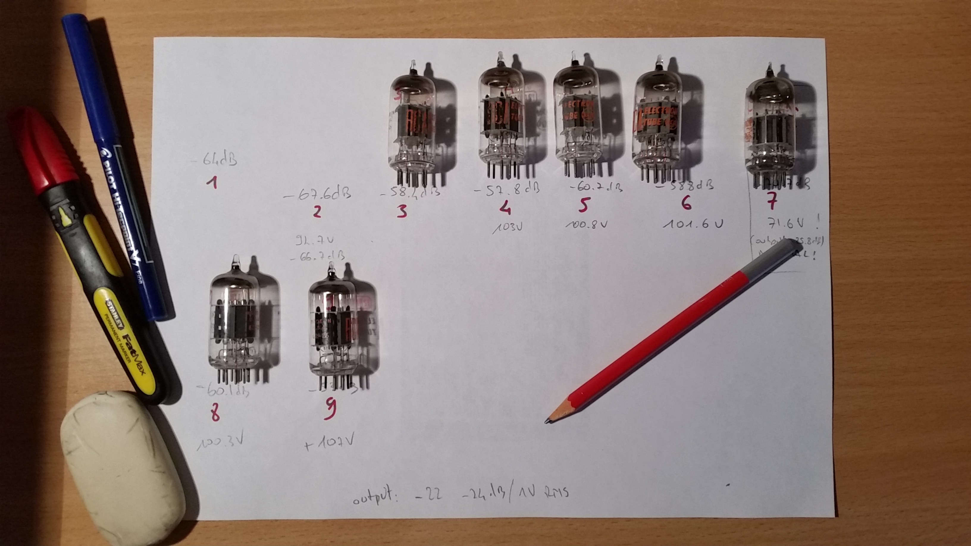
Fig. 15: Sorting ECC88/12AX7A tubes for the best THD... (click to enlarge).
From a more personal and subjective point of view, my ears are pleased by the sound of the ensemble and the preamplifier seems to be a good companion of the 55 W+55 W solid-state power amplifier I built a few years ago. As I said above, I do not think that vacuum tubes are by any means superior to their silicon counterparts. The simplest, most effective and rational solution would probably have been to adopt low-noise operational amplifiers and build a circuit around them. The power consumption would be lower of several orders of magnitude, the simplicity of the circuit would be greater and employing low voltages would have been easier. However, I like vacuum tubes and retro solutions (have you seen my Nixie clock?) and I really enjoy experimenting with them, as figure 15 attests. Even with very simple circuits like a common-cathode arrangement, the supply voltages are so high that there is a formidable amount of headroom for the signals and it is possible to tame the harmonic distortion to a very reasonable HiFi performance, especially with good tubes. If you build this circuit, I hope you will enjoy making it as much as I did.
Log:
- December 30, 2022 - Corrected typos. Added a note.
- November 15, 2020 - Corrected an error in the circuit of figure 13 (D2 badly oriented).
- January 10, 2016 - Anti-bump circuit (it, fr, en)
- June 14, 2015 - Italian translation
- June 8, 2015 - French translation
- June 2, 2015 - First version of the page, in English
License

This work is licensed under a Creative Commons Attribution-NonCommercial 4.0 International License.